Research
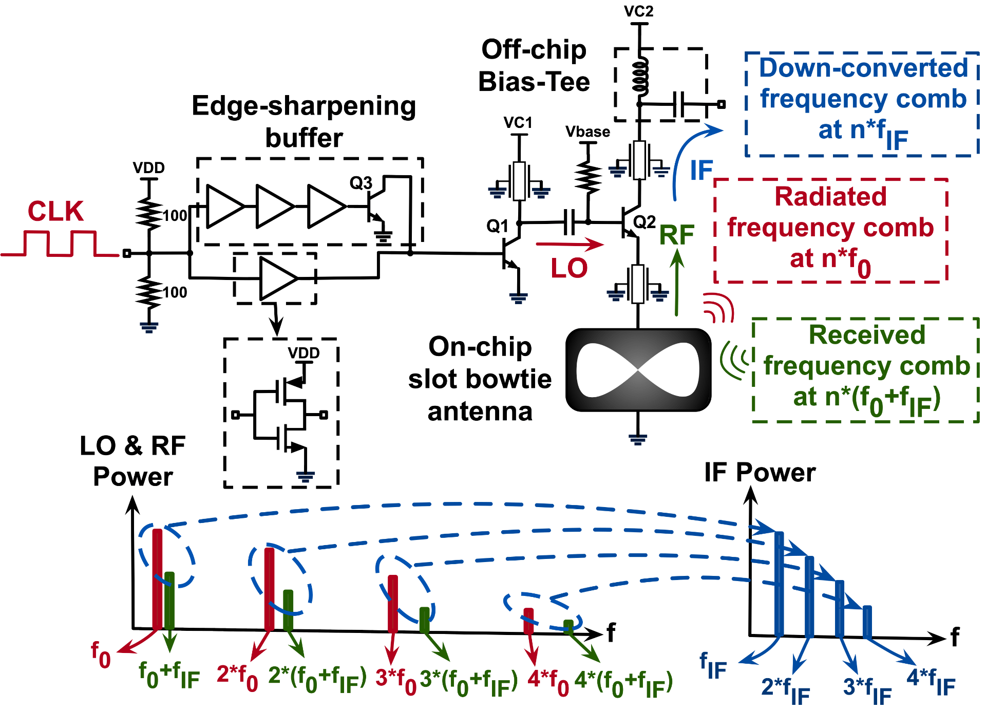
“A 400-GHz Efficient Radiator and OOK Transceiver for Multi-Gb/s Wireless Communication in Silicon,” in IEEE Journal of Solid-State Circuits, vol. 59, no. 5, pp. 1381-1397, May 2024, doi: 10.1109/JSSC.2024.3353809.

“A 0.28 THz Super-Harmonic Self-Injection-Locked Radar for Vibration Sensing and Phase Imaging,” in IEEE Microwave and Wireless Technology Letters, vol. 35, no. 4, pp. 496-499, April 2025, doi: 10.1109/LMWT.2025.3542319

“A 132-204 GHz Carrier Storage Frequency Divider with sub-50 Micro-Watt DC Power,” in 2024 IEEE BiCMOS and Compound Semiconductor Integrated Circuits and Technology Symposium (BCICTS), Oct 2024

“A Fully Integrated 20-500-GHz Coherent Detector with 2-Hz Frequency Resolution,” in 2020 IEEE BiCMOS and Compound semiconductor Integrated Circuits and Technology Symposium (BCICTS), Nov 2020.
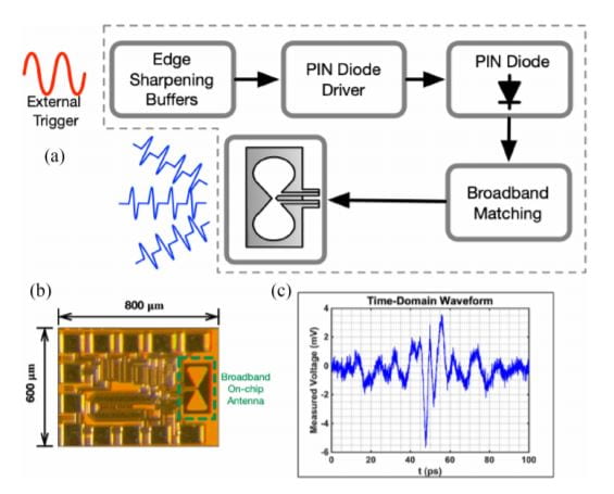
“A 4-Gb/s laser-free picosecond impulse-based wireless transmitter chip with a broadband on-chip antenna,” in 2020 45th International Conference on Infrared, Millimeter, and Terahertz Waves (IRMMW-THz), Nov 2020. 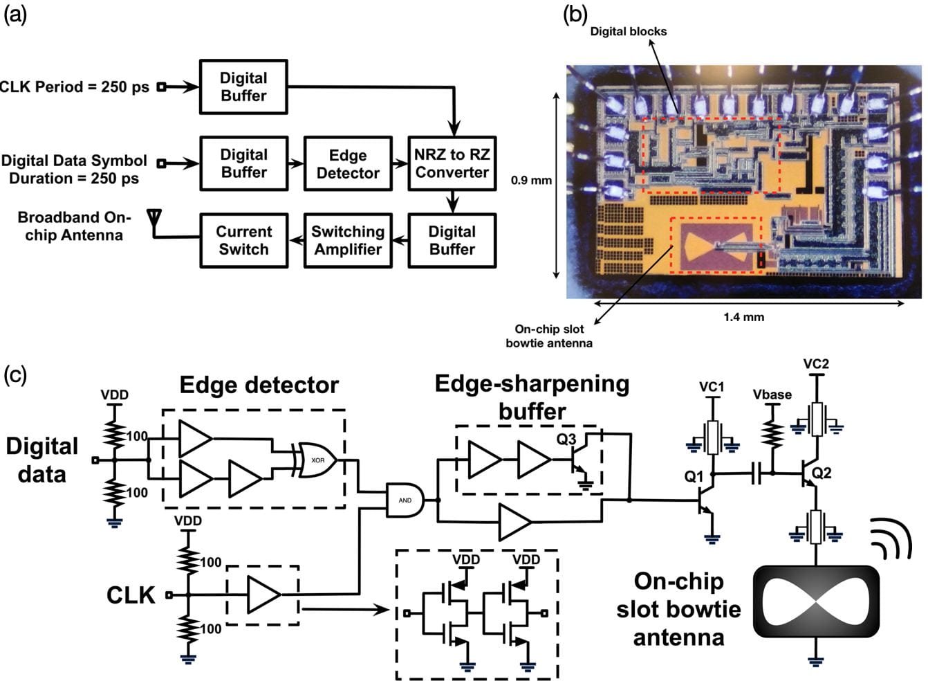
This paper presents a 4-Gb/s oscillator-free, laser-free, impulse-based transmitter for long-range wireless communication. Picosecond impulses with a full width at half maximum (FWHM) of 2.5 ps are measured, corresponding to a wideband frequency comb from 330 GHz to 1.052 THz. A specular non-line-of-sight (NLOS) link was built using this transmitter, parabolic reflector antennas, and a plane mirror. A 2-m communication link is demonstrated in this paper.
“Plasma Characterization Using a Silicon-Based Terahertz Frequency Comb Radiator,” in IEEE Sensors Letters, Sept. 2020.
different plasma parameters by varying gas pressure, plasma pulse rate, and plasma excitation power.
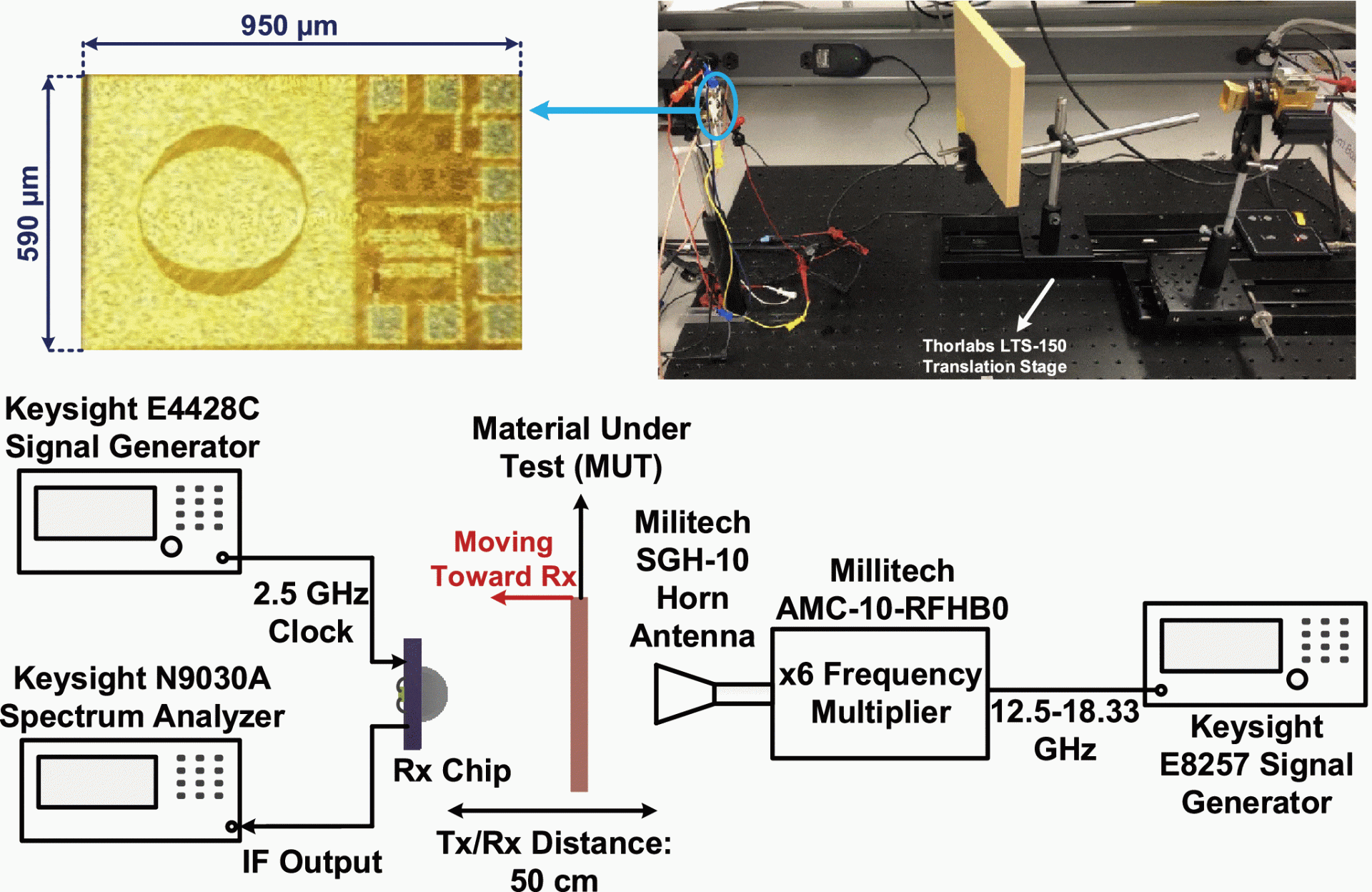
“Intelligent Material Classification and Identification Using a Broadband Millimeter-Wave Frequency Comb Receiver,” in IEEE Sensors Letters, July 2020.
“Fully electronic silicon-based THz pulse sources and detectors,” in Terahertz Photonics, March 2020.
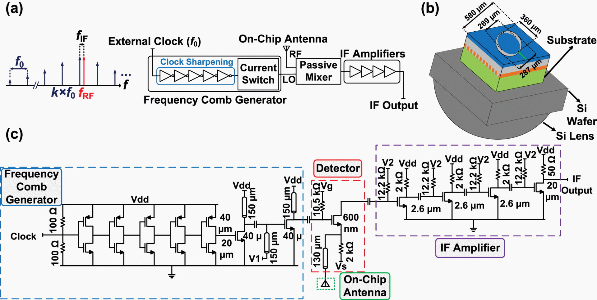
“A fully integrated 50–280-GHz frequency comb detector for coherent broadband sensing,” in IEEE Transactions on Terahertz Science and Technology, Sept. 2019.
“Wireless time transfer with subpicosecond accuracy based on a fully integrated injection-locked picosecond pulse detector,” in IEEE Transactions on Microwave Theory and Techniques, Aug. 2019.
“A self-mixing picosecond impulse receiver with an on-chip antenna for high-speed wireless clock synchronization,” in IEEE Transactions on Microwave Theory and Techniques, Feb. 2018.

“Broadband oscillator-free THz pulse generation and radiation based on direct digital-to-impulse architecture,” in IEEE Journal of Solid-State Circuits, Aug. 2017.
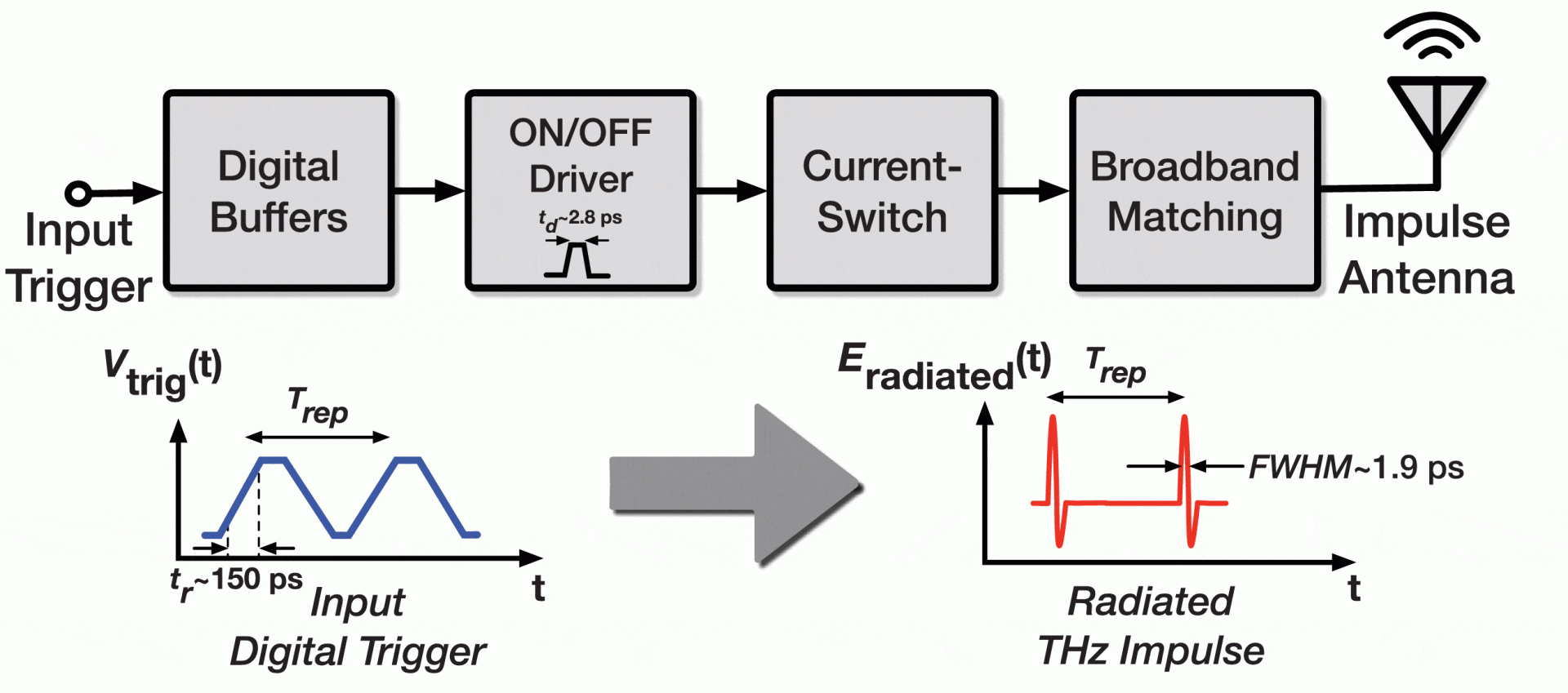
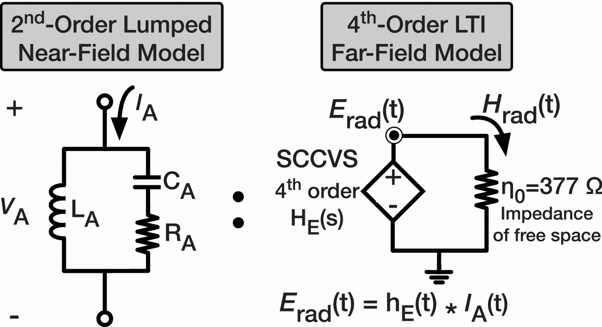
Broadband 0.03-1.1 THz signal generation and radiation are demonstrated based on an oscillator-free direct digital-to-impulse architecture with a 1.9-ps full width at half maximum and 130-GHz 3-dB bandwidth (BW) (200-GHz 10-dB BW) centered at 160 GHz. The radiated pulse achieves a peak pulse effective isotropic-radiated power of 19.2 dBm and peak pulse-radiated power of 2.6 mW. An ON/OFF impulse-shaping technique is introduced and implemented to suppress undesired ringing and to increase dc-to-radiated efficiency. The frequency-comb spectrum of the radiated pulse train with 5.2-GHz repetition rate is measured up to 1.1 THz. At a distance of 4 cm, the measured received SNR at 1 and 1.1 THz is 28 and 22 dB, respectively. A 1.1-THz tone is measured with a 10-dB spectral width of 2 Hz, demonstrating an extremely narrow spectral line width (two parts per trillion). Time-domain picosecond pulses are characterized using a custom femtosecond-laser-based terahertz time-domain spectroscopy system. Coherent spatial combining from two widely spaced chips is demonstrated. It is shown that the starting time of the radiated pulses is locked to the edge of the input digital trigger with a timing jitter of 270 fs. The chip is fabricated in a 130-nm SiGe BiCMOS process technology.
“3-D radar imaging based on a synthetic array of 30-GHz impulse radiators with on-chip antennas in 130-nm SiGe BiCMOS,” in IEEE Transactions on Microwave Theory and Techniques, Apr. 2017.
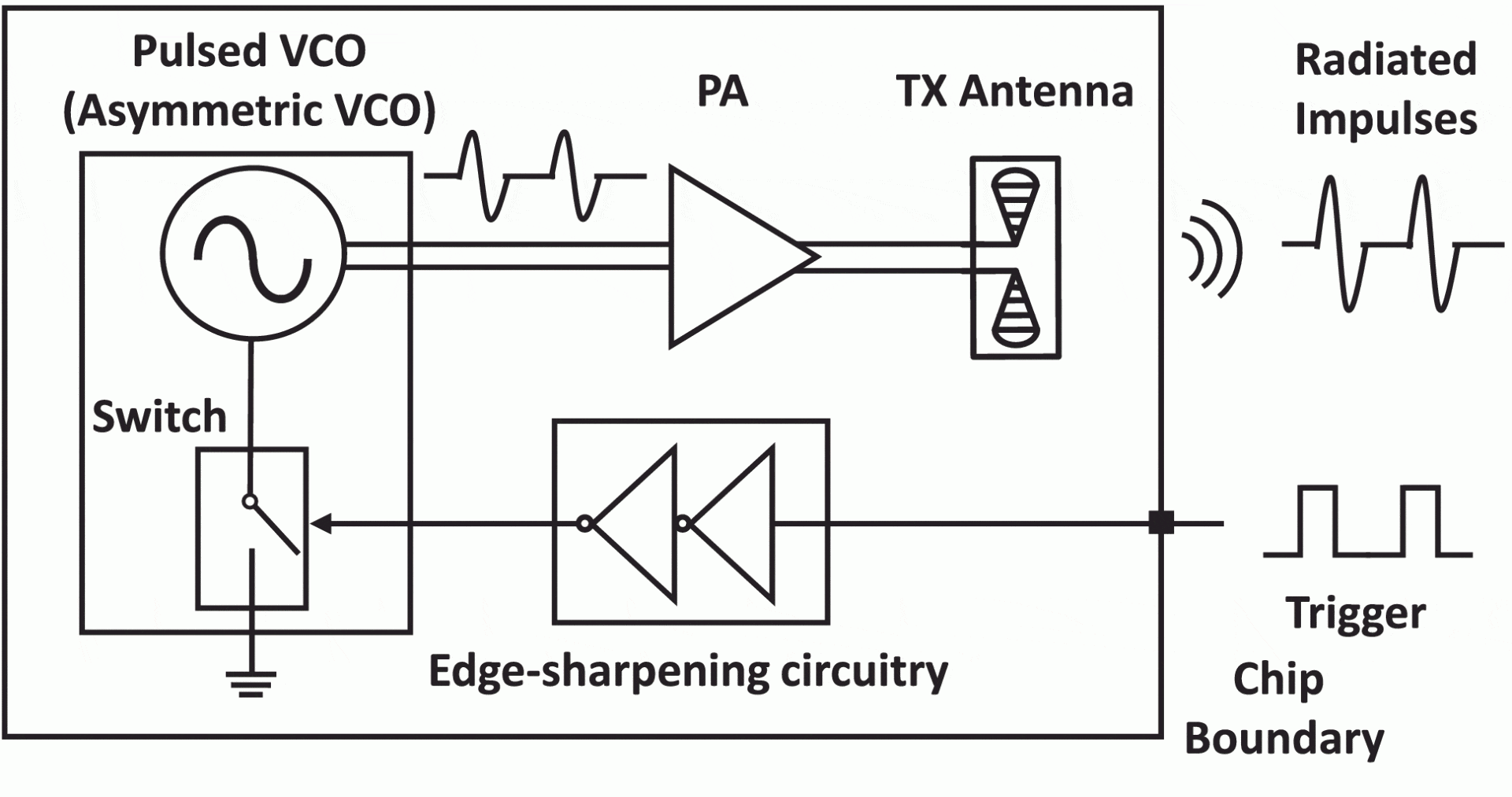
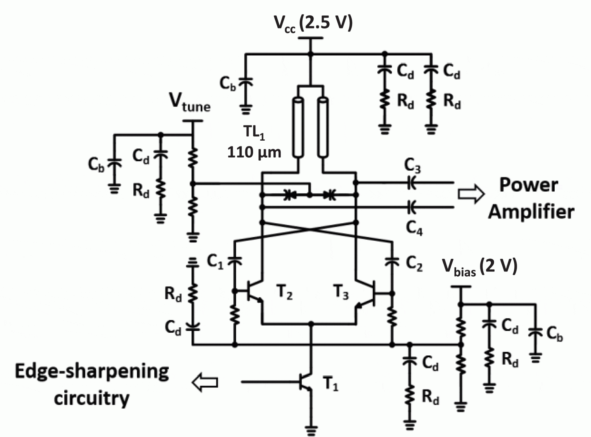
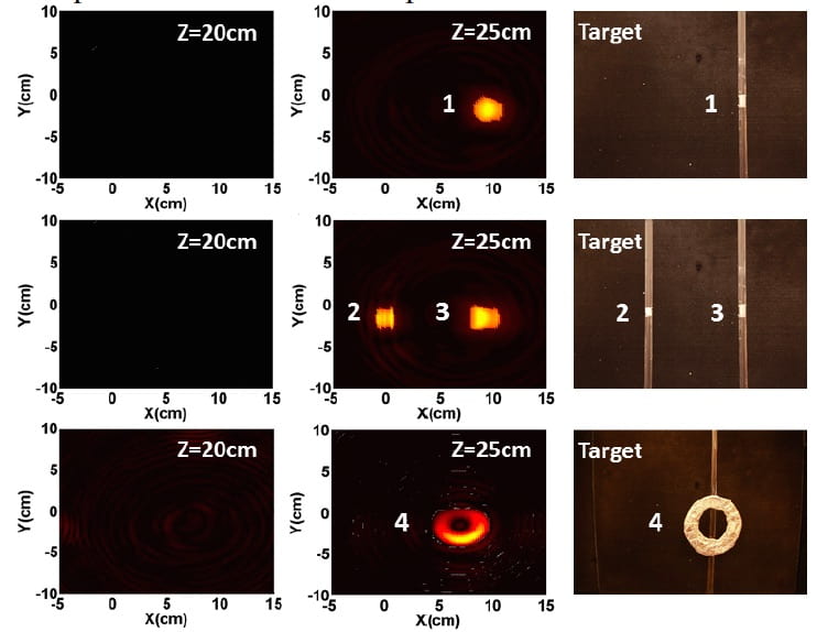
We report a 30-GHz impulse radiator chip for high-resolution 3-D radar imaging. In this paper, an asymmetrical topology in the cross-coupled pulsed VCO is introduced to minimize timing jitter of radiated impulses to 178 fs, which enables highly efficient spatial combining. The coherent combining over the air has been performed with two widely spaced impulse radiators. The shortest full-width-at-half-maximum pulsewidth of 60 ps is recorded. 3-D images of various metallic objects and dielectric objects are produced using a custom-designed synthetic array imaging system. A depth resolution of 9 mm and a lateral resolution of 8 mm at a range of 10 cm have been achieved. The impulse radiator was implemented in a 130-nm SiGe BiCMOS process technology with an area of 2.85 mm 2 and an average power consumption of 106 mW.
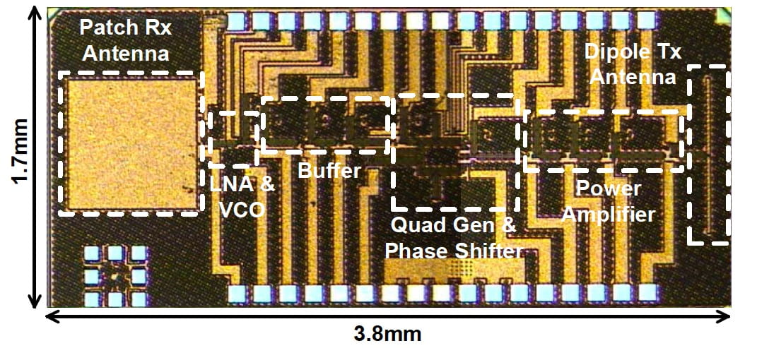
“Wireless synchronization and spatial combining of widely spaced mm-wave arrays in 65-nm CMOS,” in IEEE Transactions on Microwave Theory and Techniques, Apr. 2017.
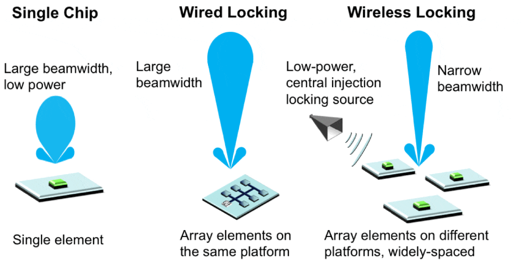
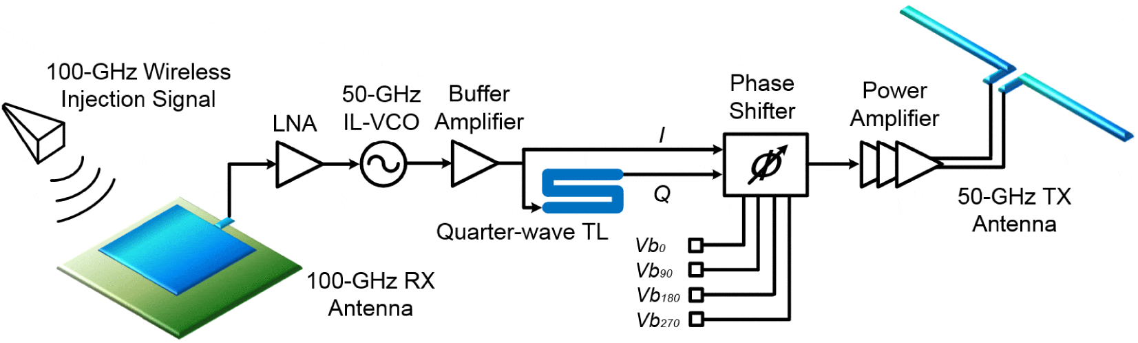
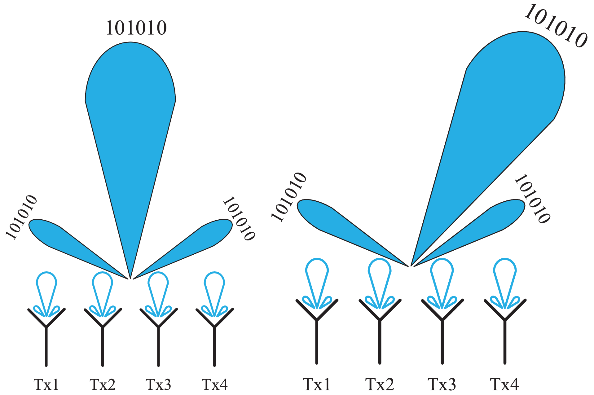
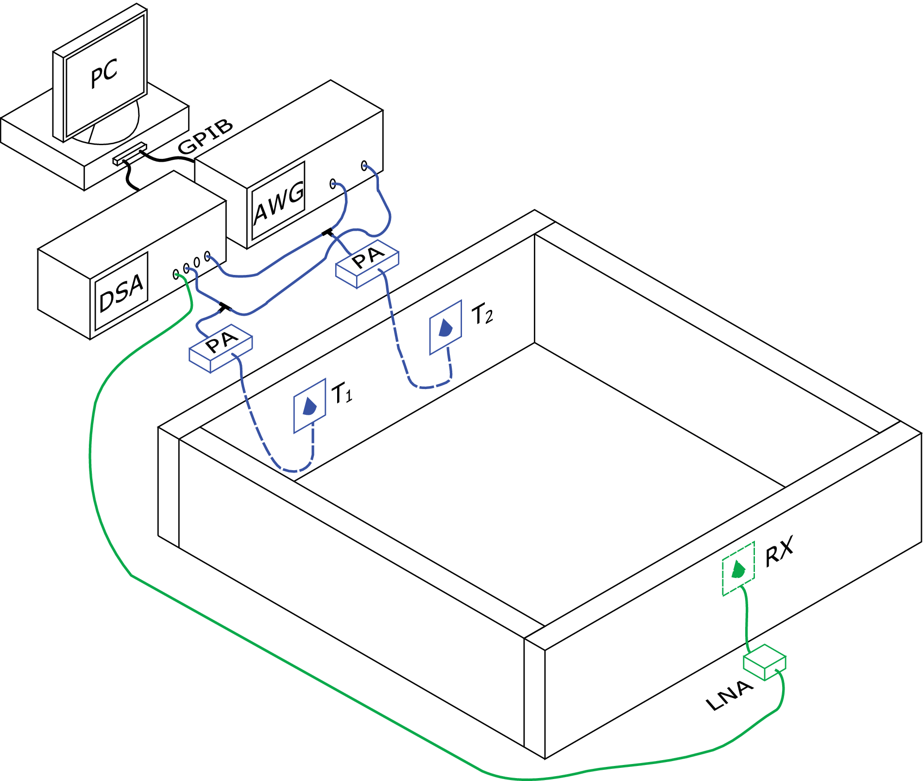
This paper presents the first wirelessly synchronized multichip array (WSMA) in 65-nm CMOS. The proposed architecture makes use of a central wireless signal to synchronize an mm-wave array, eliminating the need for connecting wires between the array elements. Wireless injection locking of a single chip is successfully demonstrated, and a 3-dB linewidth of 400 Hz at a carrier frequency of 50 GHz is achieved (stability ratio of 8 ppb). In addition, a two-element WSMA with an array aperture greater than 20 wavelengths is demonstrated using the proposed transceiver architecture. The reported transceiver includes a receiving on-chip antenna, a low-noise amplifier, an injectionlocked voltage-controlled oscillator, a buffer amplifier, an in-phase/quadrature generator, a phase shifter, a power amplifier, and a transmitting on-chip antenna. The chip is fabricated in a 65-nm CMOS process and occupies an area of 1.7 mm × 3.8 mm. This paper sets the foundation for increasing the array aperture through wireless injection locking, extending traditional array systems into the high-resolution, narrow-beamwidth regime.
“Ultra-wideband joint spatial coding for secure communication and high-resolution imaging,” in IEEE Transactions on Microwave Theory and Techniques, Feb. 2017.

This paper introduces new techniques for ultra-wideband (UWB) joint spatial coding in order to establish a secure line-of-sight wireless communication link, performing precision localization of point objects, and generating high-resolution images from complex scenes. For the proposed technique, symbol generation and coding are jointly performed by multiple widely spaced transmitters. This method enables the transmission of directionally modulated signals that can only be decoded at a desired angle, resulting in a secure communication link. It is also shown that joint spatial coding by multiple transmitters that are synchronized with each other enables the precise localization of multiple point objects and allows high-resolution 3-D imaging of distributed objects. The technique is demonstrated experimentally in the frequency range 3–10 GHz by generating and detecting UWB pulses.
“Gone in a Picosecond: Techniques for the Generation and Detection of Picosecond Pulses and Their Applications,” in IEEE Microwave Magazine, 2016.
This paper provides an overview of our recent work on silicon-based THz pulse technology and their applications.
“A Nonlinear Q-Switching Impedance Technique for Picosecond Pulse Radiation in Silicon,” in IEEE Transactions on Microwave Theory and Techniques, 2016.
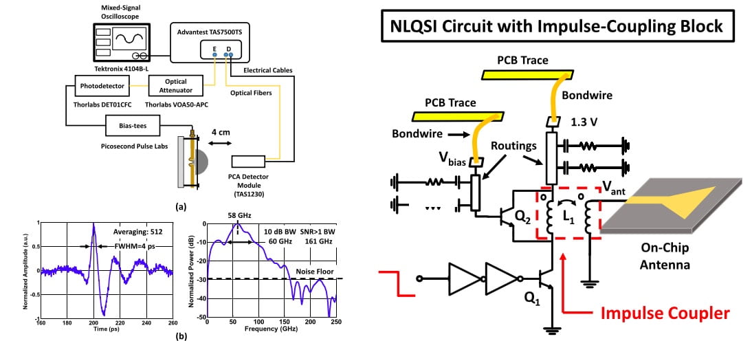
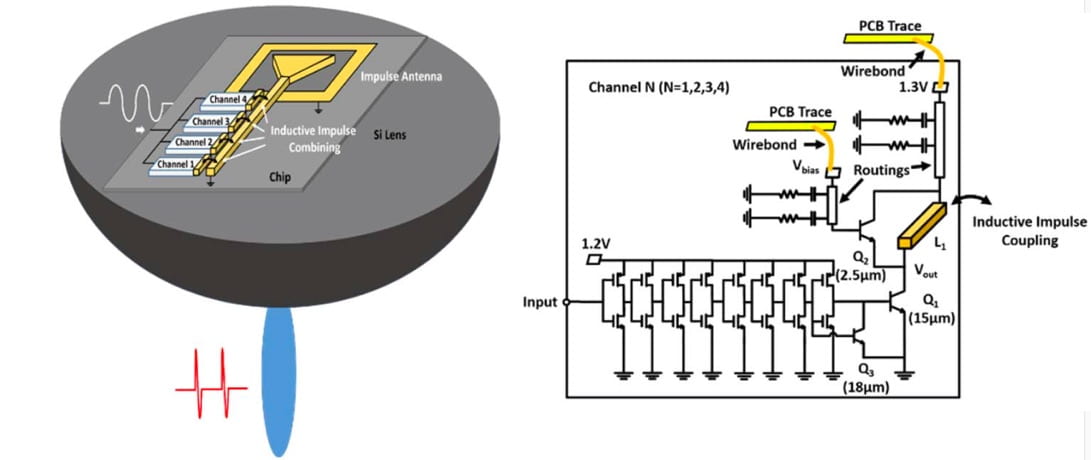
This paper presents a nonlinear Q-switching impedance (NLQSI) technique for picosecond pulse radiation in silicon. A prototype chip is designed with four NLQSI-based impulse generation channels, which can produce picosecond pulses with a reconfigurable amplitude. An on-chip impulse-coupling scheme combines the outputs from four channels and delivers the combined signal to an on-chip antenna. In addition, an asynchronous optical-sampling measurement system is used to characterize the radiated picosecond pulses in the time domain. The prototype chip can radiate 4ps pulses with an SNR > 1 bandwidth of 161 GHz. Furthermore, pulse amplitude modulation is experimentally demonstrated. The prototype chip is fabricated in a 130nm SiGe BiCMOS process technology with a die area of 1 mm2.
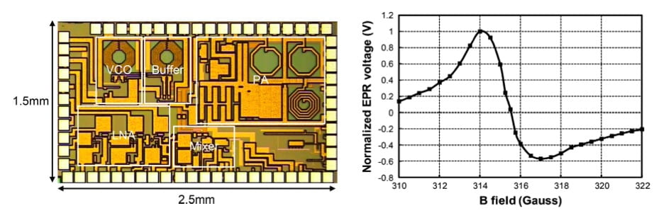
“A Full-Duplex Single-Chip Transceiver with Self-Interference Cancellation in 0.13µm SiGe BiCMOS for Electron Paramagnetic Resonance Spectroscopy,” in IEEE Journal of Solid State Circuits, 2016.
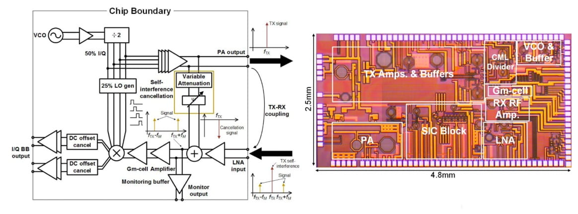
This paper presents a miniaturized EPR spectrometer based on a single-chip transceiver. Utilizing a novel on-chip self-interference cancellation circuit, the electromagnetic coupling from the transmitter (TX) to the receiver (RX) is minimized, allowing simultaneous achievement of large TX output power and low RX noise figure (NF). In the measurement, the RX achieves a NF of 3.1 dB/6.3 dB at 10 MHz/50 kHz baseband frequencies, when the TX and cancellation circuits are turned off. The measured flicker noise corner is 60 kHz, more than 10× lower than the prior work. Moreover, for the first time, the operation of the RX and cancellation circuit is demonstrated when a co-integrated TX is operating at the same time and frequency, while producing >20 dBm output power. When the TX and cancellation circuits are turned on, at -10 dBm interference power, the measured NF is 6.8 dB/11.1 dB at 10 MHz/50 kHz baseband frequencies. This is lower by 5.6 dB/9.6 dB at 10 MHz/50 kHz baseband frequencies, compared to the NF with the cancellation circuit off at the same interference power. The transceiver chip is implemented in IBM 0.13 µm BiCMOS process and consumes a power of 2 W. Utilizing this transceiver, an electron paramagnetic resonance (EPR) spectrometer is built and tested. It is observed, through measurement, that the interference cancellation circuit increases the signal-to-noise ratio (SNR) of the EPR signal by 7 dB at -10 dBm interference power. Compared to prior work, the reported EPR spectrometer improves the sensitivity of the system by 25 dB.
“Broadband THz Spectroscopic Imaging based on a Fully Integrated 4×2 Digital-to-Impulse Radiating Array with a Full-Spectrum of 0.03-1.03THz in Silicon,”
in IEEE Symposia on VLSI Technology and Circuits, Jun. 2016.
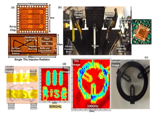
This paper presents a broadband THz frequency-comb spectroscopic imager based on a fully-integrated 4×2 picosecond Direct Digital-to-Impulse (D2I) radiating array. By employing a novel trigger-based beamforming architecture, the chip performs coherent spatial combining of broadband radiated pulses and achieves an SNR>1 BW of 1.03THz (at the receiver) with a pulse peak EIRP of 30dBm. Time-domain radiation is characterized using a fsec-laser-based THz sampler and a pulse width of 5.4ps is measured. Spectroscopic imaging of metal, plastic, and cellulose capsules (empty and filled) are demonstrated. This chip achieves signal generation with an available full-spectrum of 0.03-1.03THz. The 8-element single-chip array is fabricated in a 90nm SiGe BiCMOS process.
“Broadband Beam-forming of Terahertz Pulses with a Single-Chip 4×2 Array in Silicon,” in IEEE Antennas and Propagation International Symposium, Jun. 2016.(Best Paper Award-2nd Place)

In this paper, a single-chip impulse antenna array is presented that performs spatial combining of picosecond impulses radiated from 8 elements. A new broadband beamforming architecture is introduced that controls the timing of impulses radiated from each antenna by delaying a trigger signal, with resolution steps of 300fsec. This method eliminates the distortive and narrowband effects of delay blocks in conventional phased arrays by separating the delay path from the information path. Frequency domain measurements are performed up to 1.03THz and array directivities of 22dBi at 0.33THz, 25dBi at 0.57THz, and 27dBi at 0.75THz are achieved. The 8-element array is fabricated in a 90nm Silicon Germanium BiCMOS process technology.
“A 4ps Amplitude Reconfigurable Impulse Radiator with THz-TDS Characterization Method in 0.13µm SiGe BiCMOS,” in IEEE MTT-S Int. Microwave Symposium, May. 2016.(Best Paper Award-2nd Place)
This paper reports a fully integrated impulse radiator with the capability of radiating impulses with 4ps FWHM and reconfigurable amplitude. The peak radiated power at 54GHz is 8.7dBm with a 13.6dBm peak EIRP. A Non-Linear Q-Switching Impedance (NLQSI) technique is introduced to generate impulses and control their amplitudes. Furthermore, a two-bit impulse amplitude modulation is achieved through an on-chip four-way impulse combiner, which also attenuates parasitic-induced low-frequency radiation. In addition to performing frequency-domain measurements, for the first time, an ultra-wideband THz Time-Domain Spectroscopy (THz-TDS) system is utilized to characterize the radiated signal in time-domain. The radiated impulse has an SNR>1 bandwidth of more than 160GHz. The fully-integrated impulse radiator is implemented in a 0.13μm SiGe BiCMOS process. It has a die area of 1mm2 and it consumes 170mW.
“Sub-picosecond Wireless Synchronization Based on a Millimeter-Wave Impulse Receiver with an On-chip Antenna in 0.13µm SiGe BiCMOS,” in IEEE MTT-S Int. Microwave Symposium, May. 2016.
This paper presents a wireless synchronization receiver using sub-8psec pulses. A novel self-mixing technique is introduced to detect low-power picosecond impulses and extract the repetition rate with a low timing jitter. The chip is fabricated in a 0.13μm SiGe BiCMOS process and achieves a time transfer accuracy of 376fsec. The receiver, which is integrated with a broadband on-chip antenna, successfully detects a picosecond pulse train with a 3.1GHz repetition rate and generates an output locked to this rate with a phase noise of -89 dBc/Hz at 100 Hz frequency offset. The chip consumes 146 mW from a 2.5V supply and occupies an area of 1.89mm2.
“Terahertz Trace Gas Spectroscopy Based on a Fully-Electronic Frequency-Comb Radiating Array in Silicon,” in the Conference on Lasers and Electro-Optics (CELO), Jun. 2016.
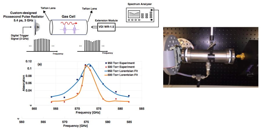
A silicon integrated circuit is reported for radiating picosecond pulses with tunable repetition rate, covering frequencies from 0.03 to 1.03 THz. This source is used in a gas spectroscopy setup to measure the absorption lines of ammonia and water in the terahertz region.
“A Fully-Integrated Digitally-Programmable 4×4 Picosecond Digital-to-Impulse Radiating Array in 65nm Bulk CMOS, “
in IEEE MTT-S Int. Microwave Symposium, May. 2016.
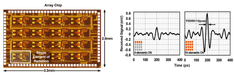
In this paper, a fully-integrated 4×4 digital-to- impulse radiating array with a programmable delay at each element is reported. Coherent spatial combining from 16 elements is successfully demonstrated. The combined signal from 16 elements achieves a jitter of 230fsec, a pulse width of 14psec, and an EIRP of 17dBm. Each array element is equipped with an 8-bit digitally-programmable delay that provides a step resolution of 200fsec and a dynamic range of 20psec. The chip is implemented in a 65nm bulk CMOS process.
“An Ultra-Wideband Impulse Receiver for sub-100fsec Time-Transfer and sub-30µm Localization,” in IEEE Radio and Wireless Symp. Dig. Papers, Jan. 2016.(Finalist for Best Paper Award)
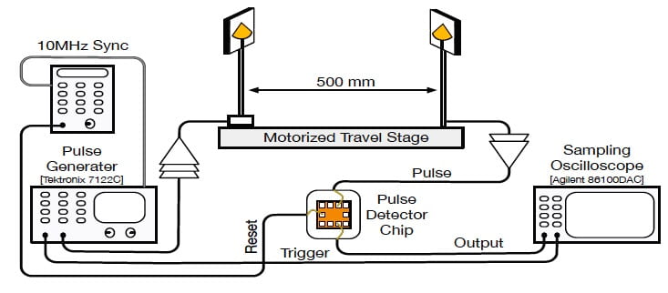
This paper presents an ultra-wideband impulse receiver capable of detecting sub-200psec pulses. The chip detects a specific zero-crossing of an incoming pulse and mitigates the undesired effects of ringing. The time detection sensitivity of the chip is limited by the jitter of the incoming pulse rather than the pulse width. A mean RMS jitter of 94fsec is recorded, which translates to the localization accuracy of sub-30µm. The chip is fabricated in IBM 130nm SiGe BiCMOS process technology.
“A 0.2-2.6GHz Instantaneous Frequency-to-Voltage Converter in 90nm CMOS,” in IEEE Radio and Wireless Symp. Dig. Papers, Jan. 2016.
“A Single-Chip Electron Paramagnetic Resonance Transceiver in 0.13µm SiGe BiCMOS,” in IEEE Transactions on Microwave Theory and Techniques, Oct. 2015.
We report the first absorption-based single-chip transceiver for electron paramagnetic resonance (EPR) spectroscopy in silicon. The chip is implemented in a 0.13µm SiGe BiCMOS process technology. The transmitter generates and delivers a continuous-wave microwave signal with a frequency range from 895 to 979 MHz and the receiver adopts a direct-conversion architecture. Based on the single-chip transceiver and a printed-circuit-board-based planar resonator, an EPR spectrometer is assembled and tested. The spectrometer successfully measures the EPR response from samples including 2,2-Diphenyl-1-Picrylhydrazyl powder, Fe3O4 nanoparticles, and Fe2O3 nanoparticles.
“Wireless Synchronization of mm-wave Arrays in 65nm CMOS,” in IEEE CICC Symp. Dig. Papers, Sept. 2015.
This paper presents the first wireless synchronization of a mm-wave array, eliminating the need for connecting wires between the array elements. Wireless
injection locking is successfully demonstrated and a 3dB bandwidth of 400Hz at a carrier frequency of 50GHz is achieved (frequency stability of 8ppb). The chip includes two on-chip antennas, a power amplifier, a phase-shifter, buffer amplifiers, and a VCO. The chip is fabricated in a 65nm CMOS process and occupies an area of 1.7mm x 3.8mm.
“A 4.6-5.35GHz Transceiver with 38dB On-Chip Self-Interference Cancelation at 10kHz Offset Frequency,” in IEEE RFIC Symp. Dig. Papers, May 2015. (Finalist for Best Paper Award))

A 4.6-5.35GHz transceiver with active self interference cancelation is reported. The active cancelation circuit cancels up to 38dB of TX leakage at 10kHz offset
from the RX signal. It increases the interference P1dB from -25dBm to -8dBm, and RX gain by 15dB. When the transceiver is utilized in a magnetic resonance spectroscopy system, the SNR improves by 15dB. Furthermore, in addition to the traditional method of B0-sweep, for the first time, the method of frequency-sweep is demonstrated.
“A 30GHz Impulse Radiator with On-Chip Antennas for High-Resolution 3D Imaging,”
in IEEE Radio and Wireless Symp. Dig. Papers, Jan. 2015. (Best Paper Award)
This paper reports a 30-GHz impulse radiator utilizing an injection-locked asymmetric cross-coupled voltage-control-oscillator (VCO) with on-chip bow-tie antennas. The impulse radiator converts a digital trigger signal to a radiated impulse with a variable pulse-width down to 60psec with peak EIRP of 15.2dBm without using any lens. Coherent spatial pulse combining is demonstrated by using two widely spaced radiators. A timing jitter of the 216fsec for the combined signal is measured. The impulse radiator has the capability of producing 3D images with depth resolution of 33um at 25cm of target distance in the air. The chip is implemented in a 0.13um SiGe BiCMOS process technology. The total die area is 2.85mm2 with maximum power consumption of 106mW.
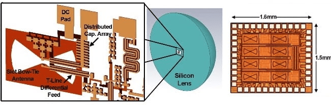
“An 8-psec 13dBm Peak EIRP Digital-to-Impulse Radiator with an On-chip Slot Bow-Tie Antenna in Silicon,” in IEEE MTT-S Int. Microwave Symposium, Jun. 2014. (Best Paper Award)
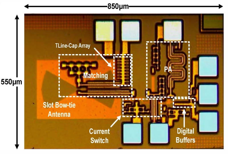
In this paper, a direct digital-to-impulse transmitter is implemented that radiates impulses with EIRP of 13dBm and a record pulse-width of shorter than 8psec. It is
shown that the starting time of the radiated impulses can be locked to the edge of the input trigger with a high timing accuracy. It is demonstrated that two widely spaced chips can generate coherent impulses in space with timing jitter of better than 270fsec. It is also shown that the frequency stability of the radiated impulses is better than 10Hz at 220GHz. The chip is fabricated in a 130nm SiGe BiCMOS process.
“A 9-psec Differential Lens-Less Digital-to-Impulse Radiator with 150-fs-Resolution Delay Line in Silicon,”
in IEEE RFIC Symp. Dig. Papers, Jun. 2014.
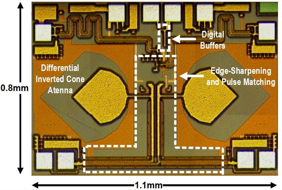
In this paper, a lens-less digital-to-impulse radiator is implemented that radiates impulses with EIRP of 10dBm and a record pulse-width of shorter than 9psec using an on-chip differential inverted cone antenna. It is shown that the starting time of the radiated impulses can be locked to the edge of the input trigger with high timing accuracy. A digitally programmable delay line is implemented and used at the input of the radiator. The delay line has a resolution step of 150fs and a dynamic range of 400ps. It is shown that by programming the delay line, the starting time of the radiated impulses in the air can be controlled.
“A 40GS/s Track-and-Hold Amplifier with 62dB SFDR3 In 45nm CMOS SOl,” in IEEE MTT-S Int. Microwave Symposium, Jun. 2014. (Finalist for Best Paper Award, 4th Prize)
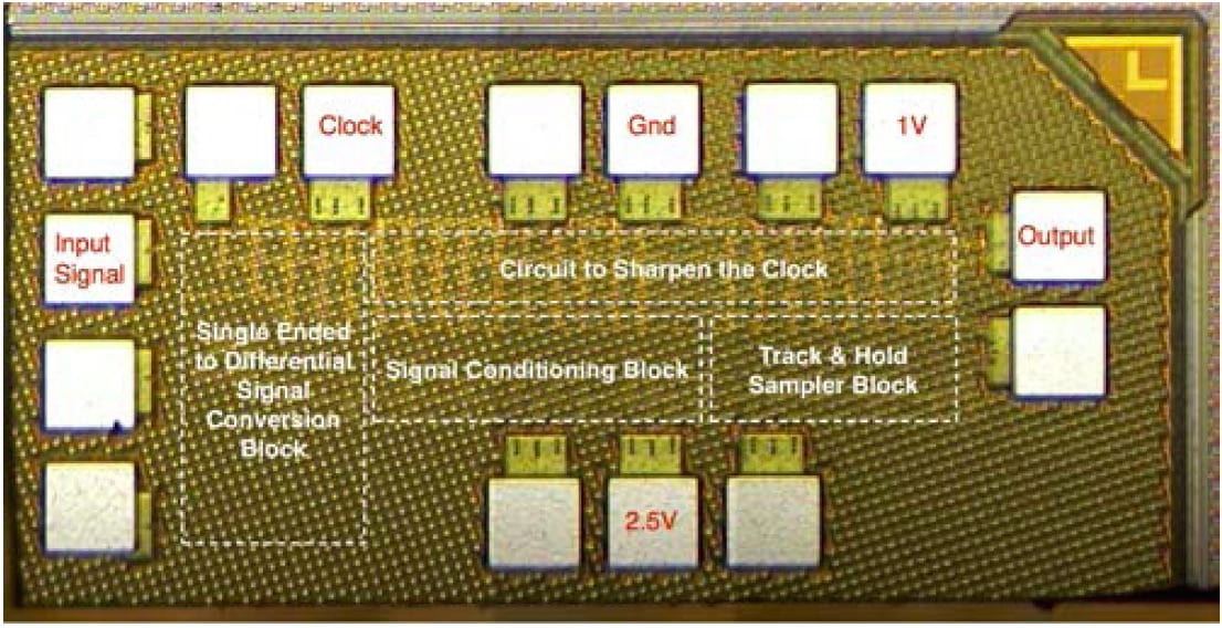
A 40GS/s Track-and-Hold amplifier with active cancellation capability is presented to mitigate the effect of leakage in transmission gate during the holding mode. A single-ended RF input signal is converted to a differential signal that feeds the active cancellation network. A record SFDR3 of 62dB with 40GS/s and SGHz input frequency is reported in 4Snm CMOS SOl. A droop voltage of 20j.lv/ns is measured. An isolation of 32dB at IGHz between the holding and tracking modes is recorded.
“A 23.5 GHz PLL with an Adaptively Biased VCO in 32 nm SOI-CMOS,” in IEEE Transactions on Circuits and Systems I: Regular Papers, vol. 60, no. 8, pp. 2009-2017, Aug. 2013.
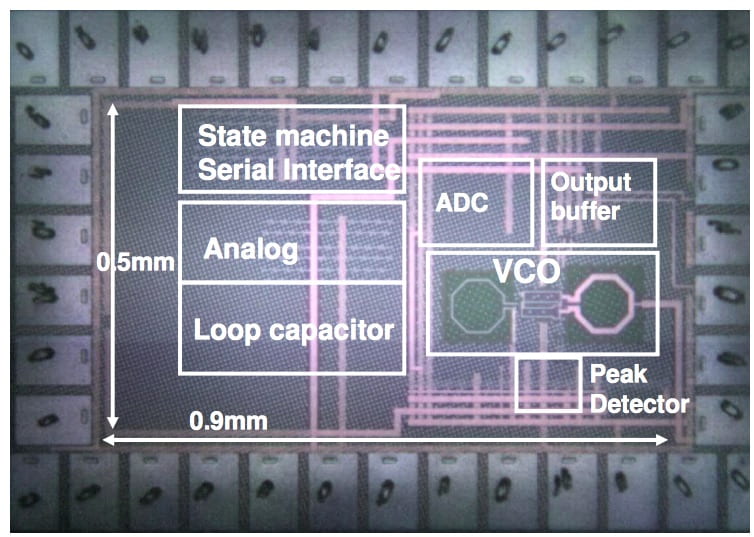
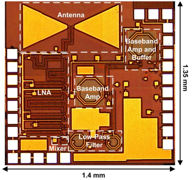
An integrated transceiver for time-domain EPR spectroscopy is implemented using a 0.13um SiGe BiCMOS technology. The system utilizes an on-chip resonator to study time domain relaxation behavior of paramagnetic samples, i.e. materials with unpaired electron spins. The single-chip EPR spectrometer consists of an EPR resonator, 22-26GHz tunable VCO, a programmable pulse generation block, RF buffer and power amplifier, a multi-stage LNA, and down-conversion mixer all in a 2mm2-size chip area.
“A Silicon-Based, Fully Integrated Pulse Electron Paramagnetic Resonance System for mm-Wave Spectroscopy, “
in IEEE MTT-S Int. Microwave Symposium, Jun. 2013.
An integrated transceiver for time-domain EPR spectroscopy is implemented using a 0.13um SiGe BiCMOS technology. The system utilizes an on-chip resonator to study time domain relaxation behavior of paramagnetic samples, i.e. materials with unpaired electron spins. The single-chip EPR spectrometer consists of an EPR resonator, 22-26GHz tunable VCO, a programmable pulse generation block, RF buffer and power amplifier, a multi-stage LNA, and down-conversion mixer all in a 2mm2-size chip area.
“A Single-Chip Dual-Mode CW/Pulse Electron Paramagnetic Resonance Spectrometer in 0.13µm SiGe BiCMOS, “
in IEEE MTT-S Int. Microwave Symposium, Jun. 2013.
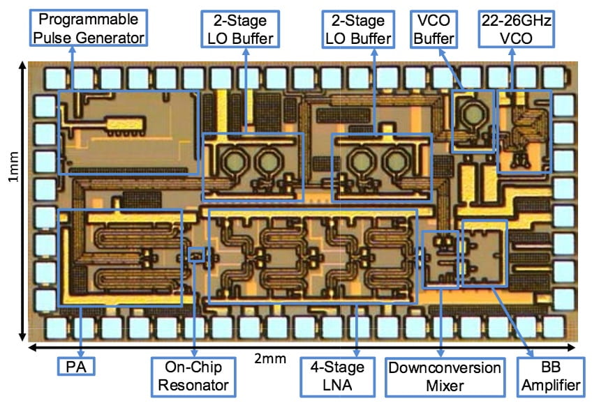
Microwave circuitry for electron paramagnetic resonance (EPR) spectroscopy is implemented in a 0.13um SiGe BiCMOS process. The chip can operate in both continuous wave (CW) and pulse modes. The frequency is tunable from 770MHz to 970MHz, corresponding to Zeeman magnetic fields from 28mT to 35mT for a free electron. The CW-EPR absorption line of a DPPH powder sample is acquired. The chip consists of a VCO, a PA, an LNA, a down-conversion mixer, baseband amplifiers, and a pulse generation block.
“A Linearized, Low-Phase-Noise VCO-based 25-GHz PLL with Autonomic Biasing,“ in IEEE J. Solid-State Circuits, vol. 48, no. 5, pp. 1138-1150, May 2013.
This paper describes a new approach to low-phase-noise LC VCO design based on transconductance linearization of the active devices. A prototype 25 GHz VCO based on this linearization approach is integrated in a dual-path PLL and achieves superior performance compared to the state of the art. The design is implemented in 32 nm SOI CMOS technology and achieves a phase noise of 130 dBc/Hz at a 10 MHz offset from a 22 GHz carrier. Additionally, the paper introduces a new layout approach for switched capacitor arrays that enables a wide tuning range of 23%. More than 1500 measurements of the PLL across PVT variations were taken, further validating the proposed design. Phase noise variation across 55 dies for four different frequencies is 0.6 dB. Also, phase noise variation across supply voltages of 0.7-1.5 V is 2 dB and across 60 temperature variation is 3 dB. At the 25 GHz center frequency, the VCO is 188 dBc/Hz. Additionally, a digitally assisted autonomic biasing technique is implemented in the PLL to provide a phase noise and power optimized VCO bias across frequency and process. Measurement results indicate the efficacy of the autonomic biasing scheme.
“An Integral Path Self-Calibration Scheme for a Dual-Loop PLL,“ in IEEE J. Solid-State Circuits, vol. 48, no. 4, pp. 996-1008 , Apr. 2013.
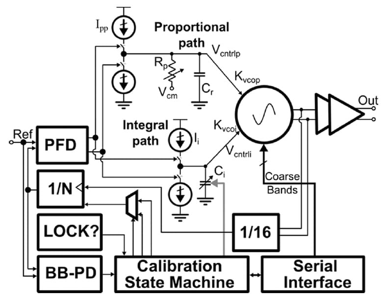
An integral-path self-calibration scheme is introduced as part of a 20.1 GHz to 26.7 GHz low-noise PLL in 32 nm CMOS SOI. A dual-loop architecture in combination with an integral path measurement and correction scheme desensitizes the loop transfer function to the VCO’s small signal gain variations.
The spread of gain peaking is reduced by self-calibration from 2.4 dB to 1 dB, when measured at 70 sites on a 300 mm wafer. The PLL has a measured phase noise @10 MHz offset of 126.5 dBc/Hz at 20.1 GHz and 124.2 dBc/Hz at 24 GHz.
“An Integral Path Self-calibration Scheme for A 20.1-26.7GHz Dual-loop PLL in 32nm SOI CMOS,” in IEEE Symposia on VLSI Technology and Circuits (VLSI), Jun. 2012, pp. 176-177.
In this paper, a bandwidth self-calibration scheme is introduced as part of a 20.1GHz to 26.7GHz, low noise PLL in 32nm CMOS SOI. A dual-loop architecture in combination with an integral path measurement and correction scheme desensitizes the loop transfer function to the VCO’s small signal gain variations. The spread of gain peaking is reduced by self-calibration from 2.4dB to 1dB, when measured at 70 sites on a 300mm wafer. The PLL has a measured phase noise @10MHz offset of -126.5dBc/Hz at 20.1GHz.
“A 21.8-27.5GHz PLL in 32nm SOI Using Gm Linearization to Achieve -130dBc/Hz Phase Noise at 10MHz Offset from a 22GHz Carrier,” in IEEE RFIC Symp. Dig. Papers, Jun. 2012, pp. 75-78 .
This paper describes a new approach to low phase-noise LC VCO design based on transconductance linearization of the active devices. A prototype 25GHz VCO based on this approach is integrated in a dual loop PLL and achieves superior performance compared to the state of the art. The design is implemented in the 32nm SOI deep sub-micron CMOS technology and achieves a phase noise of -130dBc/Hz at 10MHz offset from a 22GHz carrier. Additionally, the paper introduces a new layout approach for switched capacitor arrays that enables a wide tuning range of 23%. More than 500 measurements across PVT variations validate the proposed PLL design: phase noise variation across 46 dies for 3 different frequencies is smaller than 0.6dB, across supply variation over 0.7-1.5V is 2dB and across 80C temperature variation is 2dB. At the 25GHz center frequency, the VCO FOMT is 188dBc/Hz.
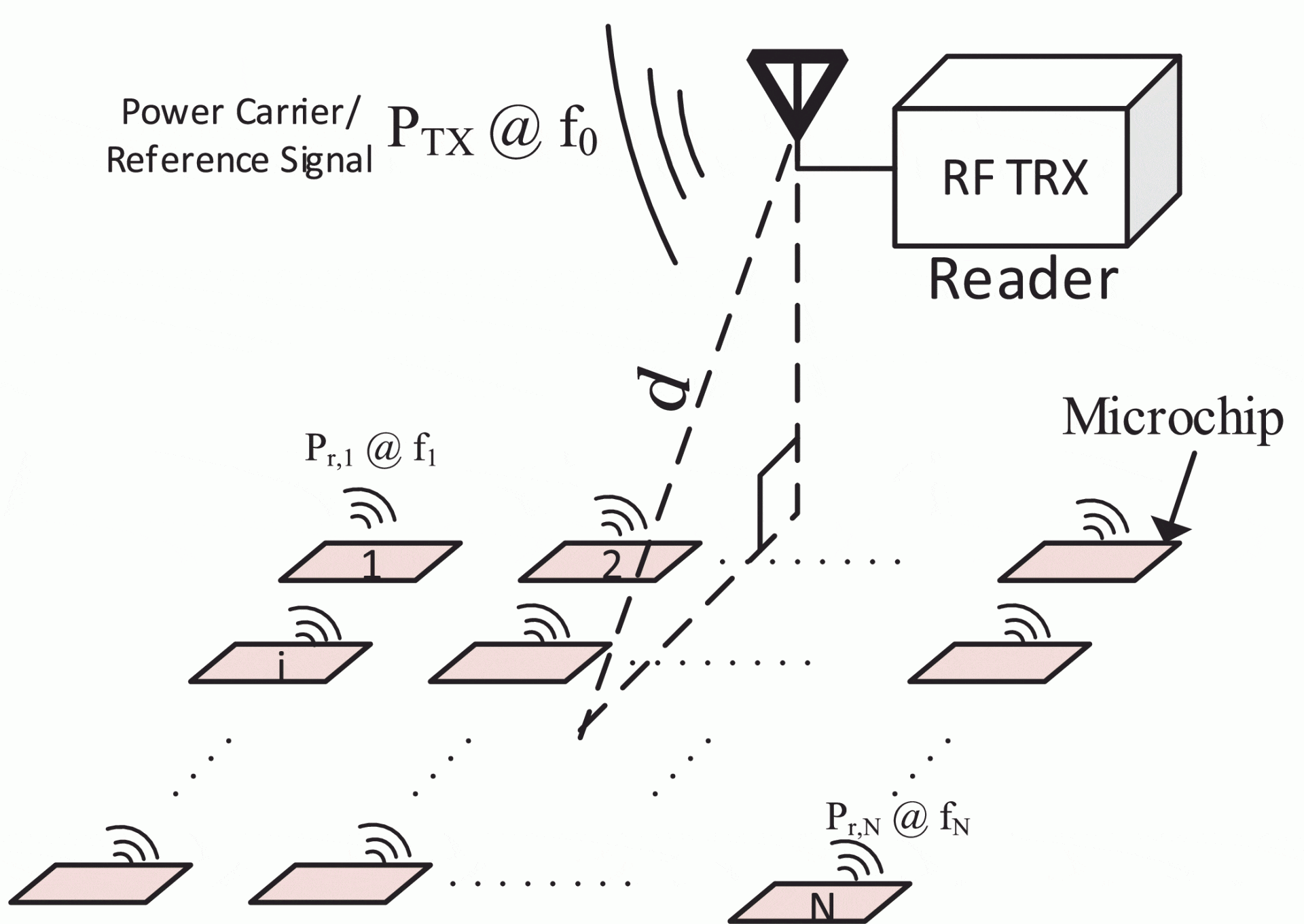
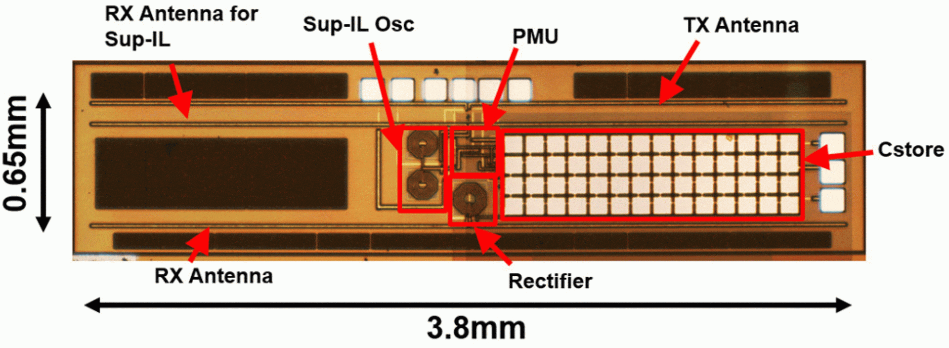
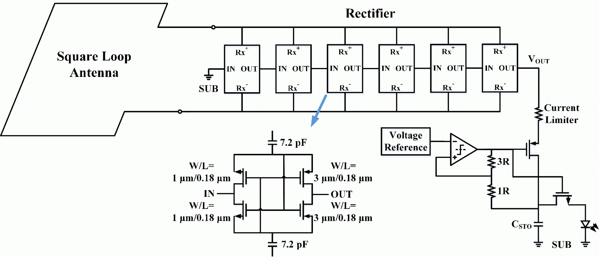
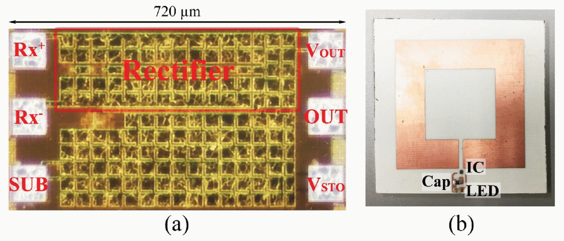
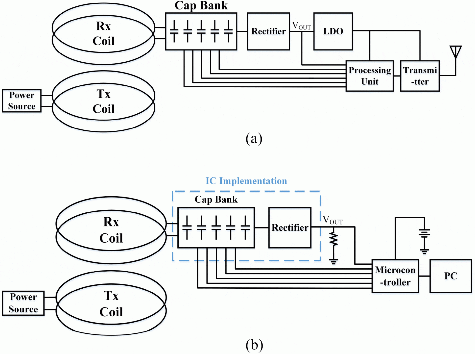
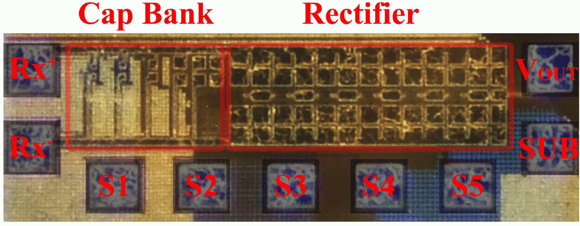
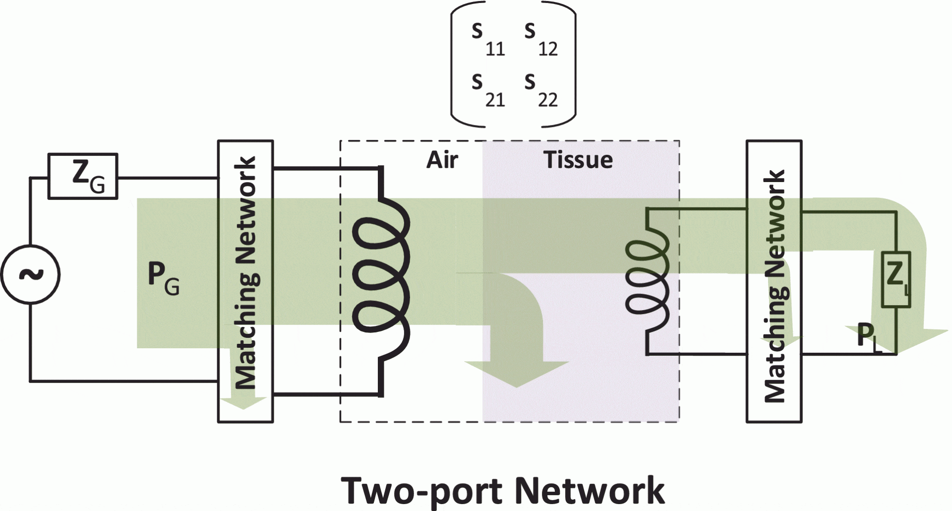
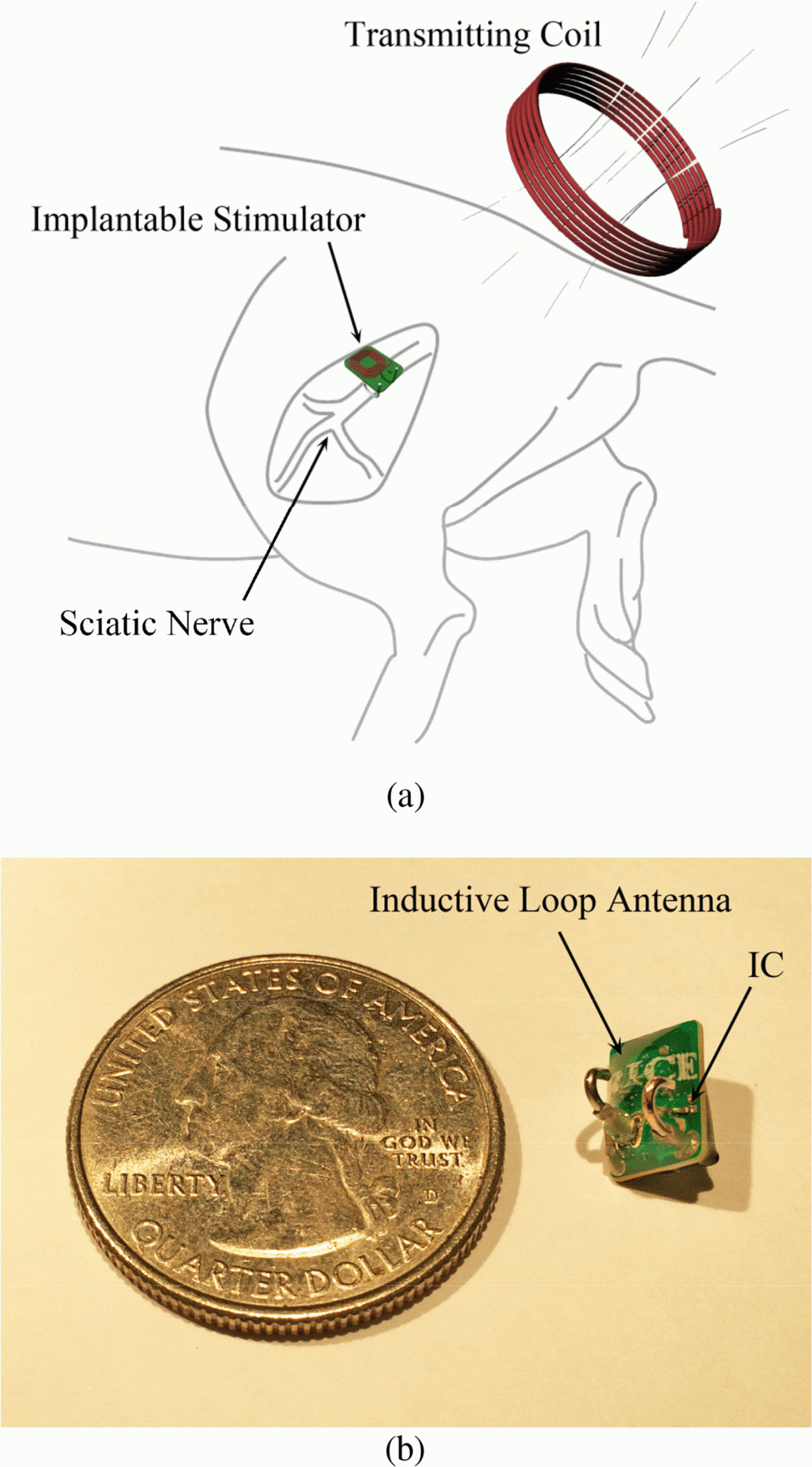
“Robust Communication and Power Transfer over a Single Loosely Coupled Inductive Link for Miniaturized and Batteryless Sensing Devices,” in IEEE Sensors Journal, doi: 10.1109/JSEN.2025.3573248.

“Towards a Machine-Learning-Assisted Dielectric Sensing Platform for Point-of-Care Wound Monitoring,” in IEEE Sensors Letters, June 2020.
“Coherent Radiation from a Swarm of Wirelessly Powered and Synchronized Sensor Nodes,” in IEEE Sensors Journal, May 2020.
“Synchronized Biventricular Heart pacing in a closed-chest porcine Model based on Wirelessly powered Leadless pacemakers,” in Scientific Reports, February 2020.


“A 100-M/s 2.6-pJ/pulse compact UWB impulse transmitter based on antenna-and-pulse-generator codesign,” in IEICE Electronics Express, Dec. 2019.
“Stretchable transparent wireless charging coil fabricated by negative transfer printing,” in ACS applied materials and interfaces, Oct. 2019.

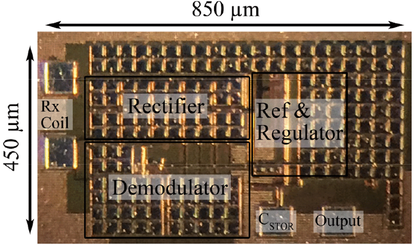
“A wirelessly powered injection-locked oscillator with on-chip antennas in 180-nm SOI CMOS for spectroscopy application,” in IEEE Sensors Letters, July 2019.

“A 915-MHz Far-Field Energy Harvester With− 22-dBm Sensitivity and 3-V Output Voltage Based on Antenna-and-Rectifier Codesign,” in IEEE Microwave and Wireless Component Letters, July 2019.
“Carbon nanotube thin film patch antennas for wireless communications,” in Applied Physics Letters, May 2019.

“Towards the implementation of a wirelessly powered dielectric sensor with digitized output for implantable applications,” in IEEE Sensors Letters, Jan. 2019.
“Wirelessly-powered dielectric sensor with on-chip antennas in 180 nm SOI CMOS process,” in IEEE Sensors Journal, Dec. 2018.

“A 430-MHz wirelessly powered implantable pulse generator with intensity/rate control and sub-1 μA quiescent current consumption,” in IEEE transactions on biomedical circuits and systems, Nov. 2018.

“A dual-mode RF power harvesting system with an on-chip coil in 180-nm SOI CMOS for millimeter-sized biomedical implants,” in IEEE Transactions on Microwave Theory and Techniques, Oct. 2018.


“An energy-efficient wirelessly powered millimeter-scale neurostimulator implant based on systematic codesign of an inductive loop antenna and a custom rectifier,” in IEEE transactions on biomedical circuits and systems, July 2018.

“High-efficiency carbon nanotube thread antennas,” in Applied Physics Letters, Oct. 2017.


Although previous research has explored the underlying theory of high-frequency behavior of carbon nanotubes (CNTs) and CNT bundles for antennas, there is a gap in the literature for direct experimental measurements of radiation efficiency. These measurements are crucial for any practical application of CNT materials in wireless communication. In this letter, we report a measurement technique to accurately characterize the radiation efficiency of λ/4 monopole antennas made from the CNT thread. We measure the highest absolute values of radiation efficiency for CNT antennas of any type, matching that of copper wire. To capture the weight savings, we propose a specific radiation efficiency metric and show that these CNT antennas exceed copper’s performance by over an order of magnitude at 1 GHz and 2.4 GHz. We also report direct experimental observation that, contrary to metals, the radiation efficiency of the CNT thread improves significantly at higher frequencies. These results pave the way for practical applications of CNT thread antennas, particularly in the aerospace and wearable electronics industries where weight saving is a priority.
“Modulation-Doped Multiple Quantum Wells of Aligned Single-Wall Carbon Nanotubes,” in Advanced Functional Materials, Feb. 2017.
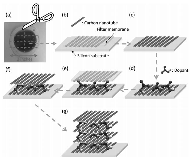

Heterojunctions, quantum wells, and superlattices with precise doping profiles are behind today’s electronic and photonic devices based on III–V compound semiconductors such as GaAs. Currently, there is considerable interest in constructing similar artificial 3D architectures with tailored electrical and optical properties by using van der Waals junctions of low-dimensional materials. In this study, the authors have fabricated a novel structure consisting of multiple thin (≈20 nm) layers of aligned single-wall carbon nanotubes with dopants inserted between the layers. This “modulation-doped” multiple-quantum-well structure acts as a terahertz polarizer with an ultra-broadband working frequency range (from ≈0.2 to ≈200 THz), a high extinction ratio (20 dB from ≈0.2 to 1 THz), and a low insertion loss (<2.5 dB from ≈0.2 to 200 THz). The individual carbon nanotube films— highly aligned, densely packed, and large (2 in. in diameter)—were produced using vacuum filtration and then stacked together in the presence of dopants. This simple, robust, and cost-effective method applies to the fabrication of a variety of devices relying on macroscopically 1D properties of aligned carbon nanotube assemblies.
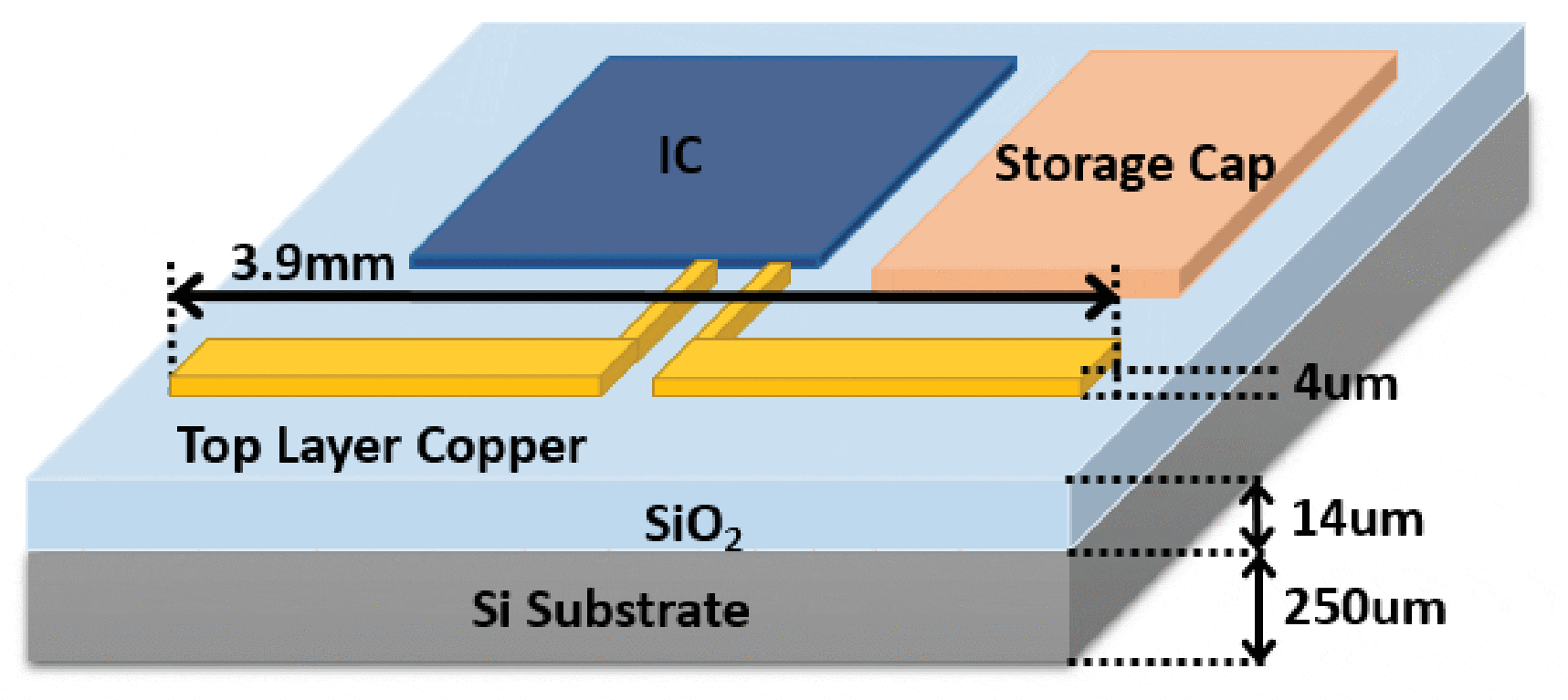
“A Fully Integrated Electromagnetic Energy Harvesting Circuit with an on-Chip Antenna for Biomedical Implants in 180 nm SOI CMOS,” in IEEE Sensors, Nov. 2016.
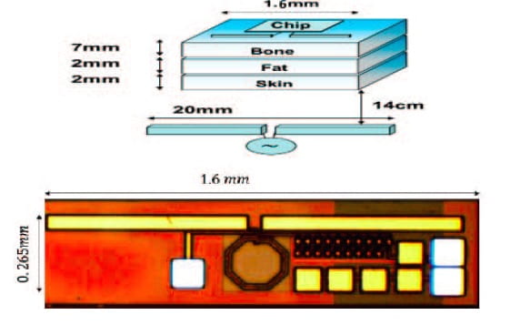
This paper presents an energy harvesting platform for biomedical implantable sensors based on a far-field electromagnetic radiation. The design is composed of an on-chip dipole antenna and a multi stage Dickson voltage rectifier with threshold compensation order of 4. The operating range is up to 15 cm, including 1 cm of biological tissue with high water content. The optimum frequency for power transmission into the implanted chip through multiple biological tissues is studied as well. The system is fabricated in a 180 nm SOI CMOS technology with a total area of 0.42 mm2. The chip can provide 1V DC for a 1MΩ resistive load when excited with an 11.2 GHz external transmitter. The maximum efficiency of the wireless link is measured as -51 dB. The voltage rectifier can provide 1V for the 1Mohm load with input power as low as 23 µW (-16.3 dBm).
“A Wirelessly Powered Injection-Locked Oscillator with On-Chip Antennas in 180nm SOI CMOS,” in IEEE MTT-S Int. Microwave Symposium, May. 2016.
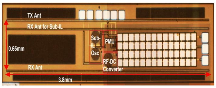
This paper presents a battery-less mm-sized wirelessly powered injection-locked oscillator with on-chip antennas in 180nm SOI CMOS. The chip harvests electromagnetic radiation from a continuous-wave source in the X-band using an on-chip antenna. In addition, the chip is equipped with a broadband injection-locking oscillator that locks to the frequency of the input and produces a synchronized signal at the half frequency of the input. The new signal is then radiated back using an on-chip dipole antenna. This architecture resolves the conventional self-interference issue in RFID sensors by separating the received and transmitted frequencies. In addition, the locking mechanism improves the phase-noise of the on-chip oscillator to -93dBc/Hz at 100Hz offset.
“Tumor Lysing Genetically Engineered T Cells Loaded with Multi-Modal Imaging Agents,” in Nature Scientific Reports, 4, Article Number: 4502, pp. 1-6, Mar. 2014.
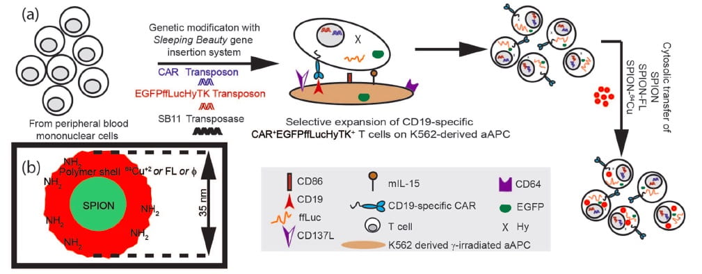
Genetically-modified T cells expressing chimeric antigen receptors (CAR) exert anti-tumor effect by identifying tumor-associated antigen (TAA), independent of major histocompatibility complex. For maximal efficacy and safety of adoptively transferred cells, imaging their biodistribution is critical. This will determine if cells home to the tumor and assist in moderating cell dose. Here, T cells are modified to express CAR. An efficient, non-toxic process with potential for cGMP compliance is developed for loading high cell number with multi-modal (PET-MRI) contrast agents (Super Paramagnetic Iron Oxide Nanoparticles – Copper-64; SPION-64Cu). This can now be potentially used for 64Cu-based whole-body PET to detect T cell accumulation region with high-sensitivity, followed by SPION-based MRI of these regions for high-resolution anatomically correlated images of T cells. CD19-specific-CAR1SPIONpos T cells effectively target in vitro CD191 lymphoma.
“In-plane heterostructures of graphene and hexagonal boron nitride with controlled domain sizes,“ in Nature Nanotechnology, pp. 119-124, Jan. 2013.
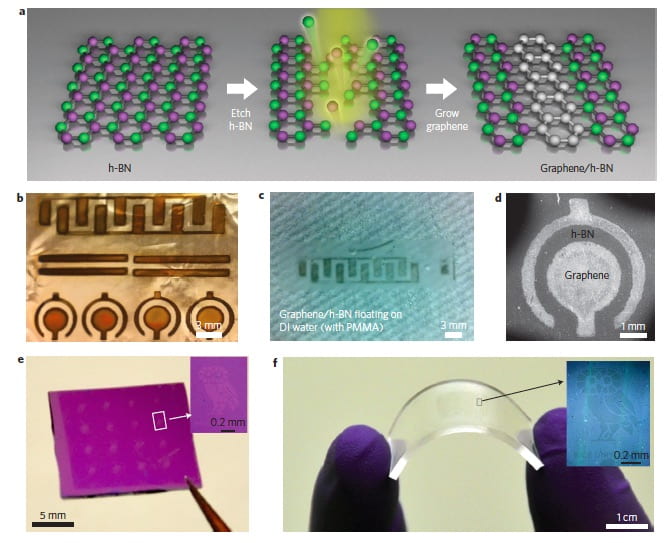
Graphene and hexagonal boron nitride (h-BN) have similar crystal structures with a lattice constant difference of only 2%. However, graphene is a zero-bandgap semiconductor with remarkably high carrier mobility at room temperature, whereas an atomically thin layer of h-BN4-9 is a dielectric with a wide bandgap of ~5.9 eV. Accordingly, if precise two dimensional domains of graphene and h-BN can be seamlessly stitched together, hybrid atomic layers with interesting electronic applications could be created. Here, we show that planar graphene/h-BN heterostructures can be formed by growing graphene in lithographically patterned h-BN atomic layers. Our approach can create periodic arrangements of domains with size ranging from tens of nanometres to millimetres. The resulting graphene/h-BN atomic layers can be peeled off the growth substrate and transferred to various platforms including flexible substrates. We also show that the technique can be used to fabricate two-dimensional devices, such as a split closed-loop resonator that works as a bandpass filter.
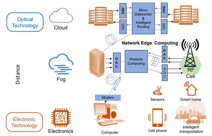
“Electronic Bottleneck Suppression in Next-generation Networks with Integrated Photonic Digital-to-analog Converters,” in arXiv, Nov. 2019.
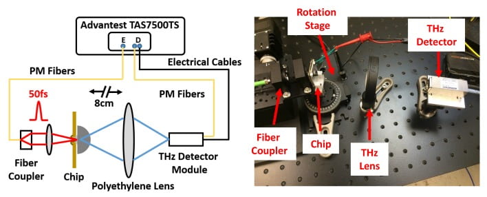
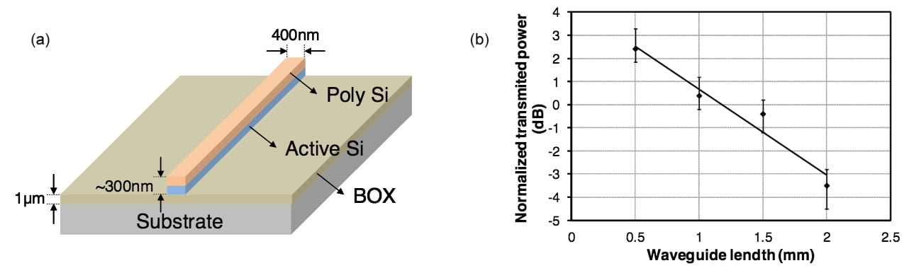
“An integrated Germanium-based THz impulse radiator with an optical waveguide coupled photoconductive switch in silicon,” in Micromachines, June 2019.

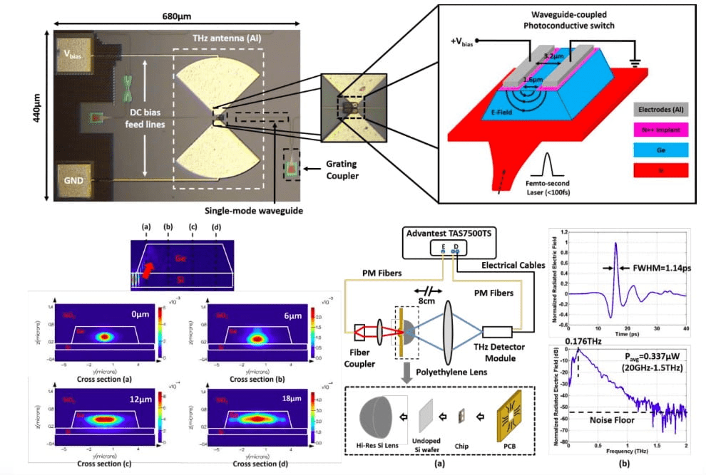
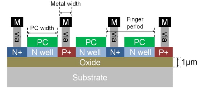
“An Integrated Germanium-Based Optical Waveguide Coupled THz Photoconductive Antenna in Silicon,” in the Conference on Lasers and Electro-Optics (CELO), Jun. 2016.
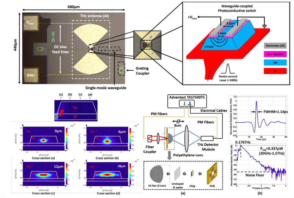
An integrated germanium-based optical waveguide coupled THz photoconductive antenna in a low-cost SOI process is presented with potentials to perform THz beam-steering. The radiated THz pulses achieve a FWHM of 1.14ps and bandwidth of 1.5THz.
“A Free-space Optically-Locked VCO with Picosecond Timing Jitter in 0.18µm CMOS,” in IEEE Photonics Technology Letters , vol. 26, no. 12, pp. 1180-1183, Jun. 2014.
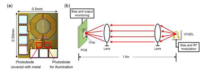
In this letter, we present a novel receiver for time transfer that achieves picosecond accuracy through a line-of-sight link. The receiver is based on a fully integrated optically locked voltage controlled oscillator (OL-VCO) and is implemented in a commercial CMOS process. The design of optical photodiodes integrated with the OL-VCO is explained in detail. It is demonstrated that in the locked mode, the OL-VCO can be synchronized with a 1.3-GHz RF source through a free-space optical link. The free-space synchronization improves the phase noise of the OL-VCO by 25 dB at 100-Hz offset frequency.
It is shown that a time transfer accuracy of picosecond can be achieved over a distance of 1.5 m. This represents more than two orders of magnitude improvement compared with the prior art.
“A 2.5Gb/s 0.38mm2 Optical Receiver with Integrated Photodiodes in 0.18µm CMOS SOI,” in IEEE MTT-S Int. Microwave Symposium, Jun. 2014.
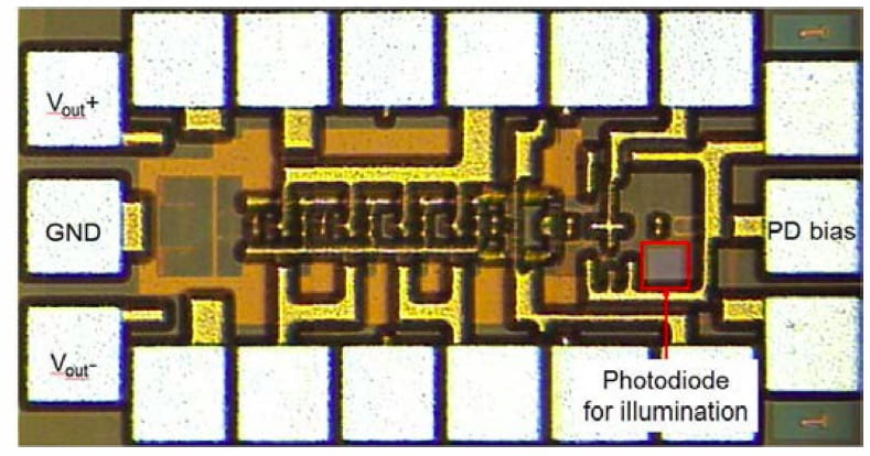
In this work, we report an optical receiver with integrated photodiodes operating at 850nm wavelength. The receiver achieves a data-rate of 2.5Gb/s without using any equalizer. To minimize the area, no inductors are used in the design. The entire receiver occupies an area of 0.38mm2. This represents the smallest optical receiver operating at the Gb/s regime. The chip is fabricated in O.18um CMOS SOl process technology.
“Picosecond Wireless Synchronization Using an Optically Locked Voltage Controlled Oscillator (OL-VCO),” in IEEE MTT-S Int. Microwave Symposium, Jun. 2014.
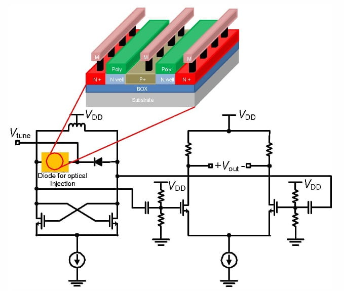
In this paper, the first fully integrated Optically Locked Voltage Controlled Oscillator (OL-VCO) is reported. The OL-VCO is locked to an RF source through a free-space optical link at 850nm. In the locked mode, the OL-VCO achieves an RMS jitter of 1.6psec with 16 averaging. It also improves the phase noise by 25dB at 100Hz offset frequency. The wireless synchronization is achieved at a distance of 1.5m, representing more than two orders of magnitude improvement compared to the prior art.
“Impact of Layout on the Performance of Photodiodes in 0.18µm CMOS SOI,“ in IEEE Photonics Conference (IPC), Sept. 2013, pp. 343-346.
The impact of layout on the responsivity and bandwidth of photodiodes is studied and summarized. The photodiodes are fabricated in a 0.18um CMOS SOI process technology. The measurements are performed at wavelengths near 850nm.
“Optical Waveguides and Photodiodes in 0.18µm CMOS SOI with No Post-processing,“ in Optical Fiber Communication (OFC) Conference, Mar. 2013
This paper demonstrates the first optical waveguide and fastest photodiode implemented in a commercial CMOS technology without performing any post-processing. The measured waveguide
loss at 1.55um is 37dB/cm and bandwidth of photodiode exceeds 9.2GHz at 850nm.